MLCC Manufacturing Process: 14 Key Steps from Ceramic Slurry to Final Testing
2026-07-19
Known as “the rice of electronics”, MLCC (Multi-Layer Ceramic Capacitor) is a core passive component stacked with alternating ceramic dielectrics and nickel electrodes for circuit decoupling, noise filtering and voltage stabilization. Demand surges across global industries: a smartphone uses over 1,000 pieces, premium EVs need 10,000+ units, while NVIDIA GB300 AI training servers adopt 8,000–12,000 high-spec MLCCs. Major application sectors cover AI computing hardware, new energy vehicles, 5G communication, consumer electronics, industrial control and medical devices, with differentiated performance standards for each scenario.
Full 14-Step MLCC Manufacturing Flow
MLCC production falls into front forming, mid sintering and back finishing phases, requiring nano-level precision control.
- Slurry Mixing: Nano barium titanate powder mixes with binders and solvents, ball-milled for 48–72 hours to avoid particle agglomeration.
- Tape Casting: Ultra-thin ceramic green sheets under 1μm are coated on polished PET film with multi-stage gradient drying to eliminate solvent residues.
- Electrode Printing: Nickel slurry is printed with ±0.5μm alignment accuracy via CCD closed-loop correction for staggered electrode patterns.
- Stacking: Hundreds to 1,600 layers are stacked in ISO Class 1 dust-free workshops; each sheet undergoes inspection to avoid multi-layer breakdown risks.
- Isostatic Lamination: 100–300MPa vacuum pressure compresses stacked blocks to remove internal air and prevent delamination.
- Precision Cutting: Chips are cut with reserved 15–20% shrinkage allowance for later high-temperature sintering.
- Debinding: Gradient heating at 200–500°C removes organics, strictly controlling residual carbon below 0.1% to avoid insulation failure.
- High-Temperature Co-firing (core barrier): Chips are sintered at 1100–1350°C under calibrated N₂-H₂-H₂O atmosphere. Manufacturers must match shrinkage curves of ceramic and nickel electrodes, while regulating oxygen partial pressure within an ultra-narrow window to stop electrode oxidation or ceramic reduction.
- Chamfering: Chips are tumbled to fully expose inner electrode terminals for stable external connection.
- Silver Termination: Chip ends are dipped with silver paste at 15–25% immersion depth to prevent SMT tombstoning defects.
- End Firing: Secondary 750–800°C firing locks silver terminals firmly to ceramic bodies.
- Ni-Sn Electroplating: Nickel barrier layer blocks solder erosion; matte tin plating suppresses tin whisker short-circuit risks.
- 100% Full Electrical Testing: Every unit is screened for capacitance, loss, insulation resistance and voltage resistance with automatic sorting by tolerance grades.
- Taping & Vacuum Packaging: CCD secondary visual inspection is implemented before moisture-proof reel packaging with traceable QR codes.
Core Advantages of Hongda HLC MLCC Series
Based on Hongda official specifications, the HLC lineup delivers all-round reliable solutions for global electronics manufacturers.
Complete product matrix: Sizes range from mini 0201 to large 2225, with four dielectric options (NP0/X7R/X5R/Y5V). Capacitance covers 0.1pF–220μF, rated voltages from 4V to 100V, and multiple tight tolerances (±1%/±5%/±10%/±20%). NP0 features ±30ppm ultra-low temperature drift for high-frequency RF equipment; X7R maintains stable performance from -55℃ to 125℃, ideal for automotive and AI server power circuits.
Applications of Hongda MLCCs
Hongda HLC MLCCs can be used in a wide range of electronic applications, including AI servers, GPU power systems, electric vehicles, BMS circuits, 5G communication equipment, smartphones, consumer electronics, industrial control systems, medical electronic devices, smart meters, IoT devices, automotive electronic modules, power supplies, and DC-DC converters.
As AI computing, new energy vehicles, 5G infrastructure, and industrial electronics continue to grow, stable MLCC supply and reliable quality control are becoming increasingly important for global manufacturers.
Standardized high-reliability structure: RoHS & REACH compliant Ag/Ni/Sn three-layer lead-free terminals, effectively resisting solder corrosion and eliminating SMT assembly defects.
Strict full-process quality control: Hongda replicates the complete 14-step precision production workflow, equipped with high-speed six-side visual inspection equipment to sustain stable mass production yield.
Customized & flexible service: Custom low-ESR variants for EV BMS and AI GPU power supply are available, alongside one-stop passive component supply and flexible batch delivery for consumer, industrial and high-reliability projects.
Backed by mature ultra-precision manufacturing technology and full-spectrum product coverage, Hongda HLC MLCCs address booming demand from AI, communication & consumer electronic industries, providing cost-effective, high-reliability multilayer ceramic capacitor solutions amid global electronic component localization substitution.
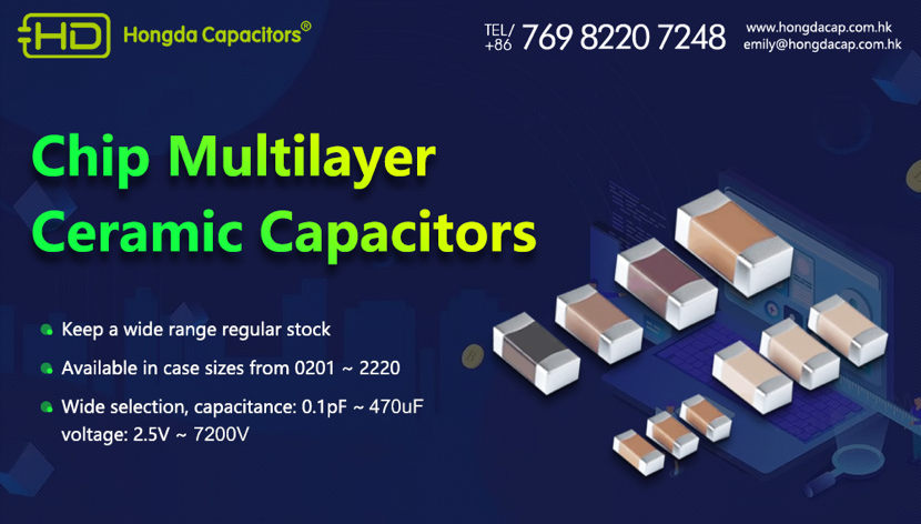
Why Choose Hongda Capacitors for MLCC Supply?
Hongda Capacitors provides MLCC solutions with broad product coverage, stable quality, and flexible supply support.
Our advantages include:
- Complete MLCC product matrix
- Multiple dielectric options for different applications
- RoHS and REACH compliant products
- Ag/Ni/Sn three-layer lead-free terminal structure
- Support for standard and customized MLCC requirements
- Stable mass production capability
- BOM matching and alternative selection support
- Flexible batch delivery for consumer, industrial, and high-reliability projects
- One-stop passive component supply
For customers facing long lead times, supply pressure, or cost challenges, Hongda Capacitors can help evaluate suitable MLCC alternatives and provide competitive sourcing support.


 English
 Chinese Simplified
 Russian
 Vietnamese
 Spanish
 Portuguese
 Arabic
 German
 Korean
 Polish
 Italian
 Turkish
 Belarusian
 Bulgarian
 Croatian
 Czech
Czech
 Danish
 Dutch
Dutch
 Estonian
 Filipino
 Finnish
 French
 Hungarian
 Indonesian
 Irish
Irish
 Japanese
 Lithuanian
 Norwegian
 Romanian
 Serbian
 Slovak
 Slovenian
 Swedish
 Thai
Thai


